AGENDA - EMC SYSTEMS ENGINEERING DESIGN SEMINAR
 EMC problems have plagued the communications/electronics industry since the late 1800's. This is significant because these early problems preceded Lee Deforest’s invention of the triode vacuum tube. When the amplification of low level signals became possible, the EMC problem became much worse because circuits could now respond to lower level interfering signals. Fortunately, there were few electronics devices to interfere, and in general they were analog! In the last 100 years, we have seen a proliferation of modulation schemes, active components, devices, and systems. Electronics is now generally digital, and generates considerable RF interference. This has resulted in the creation of laws by various governmental agencies to protect our RF environment. To cost effectively comply with these laws requires a coordinated design effort between the electronics designers, and the mechanical/packaging designers.
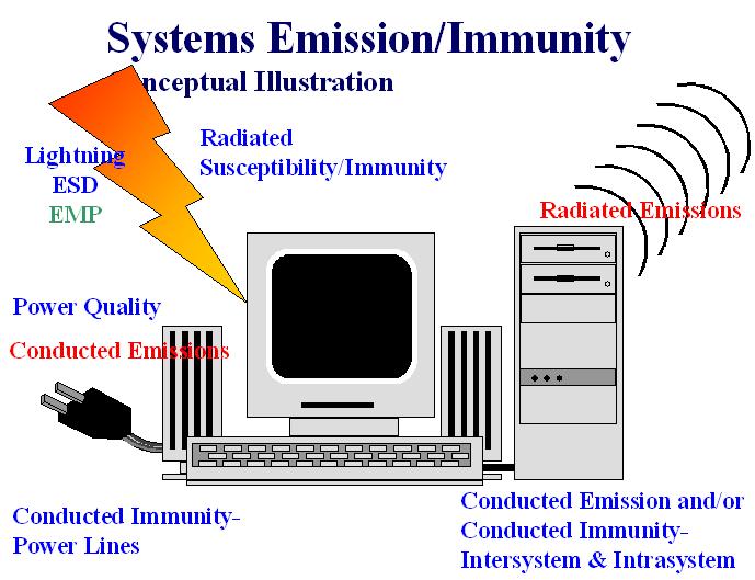
This seminar provides an overview of the EMC problem, an examination of logic EMC characteristics, and EMC systems design. The systems design presentation covers printed circuit board considerations, differential and common mode trace and cable EMC hardening, and shielding for RF emission and susceptibility (immunity) control. The emphasis will be on radiated emission from chips, interconnects, and cables; radiated susceptibility of circuits; as well as the design principles used to resolve EMC problems. The shielding discussion covers aperture controls as well as mechanical and corrosion design. Shielding design is covered in this presentation because it can be applied to existing systems without impacting signal integrity/circuit operation. It is the only suppression technique that can be used in this way.
1. OVERVIEW OF EMI/RFI/EMC PROBLEM
2. EUROPEAN EMC DIRECTIVE
Note: An overview of MIL-STD-461 can be substituted
3. SYSTEMS DESIGN
4. PCB/CABLE DESIGN PRACTICES
5. PCB/EQUIPMENT SHIELDING
6. RF GASKETS
www.ronbrewer.com