COPYRIGHT (c) 2003 - ALL RIGHTS RESERVED
Ron Brewer
RADIATED EMISSION/SUSCEPTIBILITY COUPLING LOOPS!
Most of the time, wire routing creates loops that provide paths for signal currents to move from a source to a load and then return back to the source. Loops appear within chips where they interconnect millions of transistors, on PCB's and back-planes where the trace loops are larger but there are fewer of them, and especially in cables where loop areas can be extremely large. Sometimes the loop is so ill defined that we have trouble comprehending that there really is a loop and that it is returning current to a source. This is especially true with logic circuits because they "look" so single ended! But they are loops none the less . . . and if the circuit isn't provided with a stable well defined return path; the current will return to its source the best way it can. These illusive return paths may be unacceptable because they can result in increased radiated emission from the circuit, capacitive and inductive crosstalk coupling between circuits, and increase the susceptibility of circuits closely coupled to the undefined path.
If the loop leaves the confines of the system, the unwanted RF current in the loop represents a conducted emissions problem. If the loop is directly connected to an external source of unwanted RF current then there is a potential conducted susceptibility problem. In addition, loops make good antennas (especially in the near field) that work well for both radiated emission and radiated susceptibility coupling. Handling the radiated coupling to and from the conductor is generally a more difficult EMC challenge than handling the conducted coupling problem. This mostly because conductors behave as low pass filters. It is the radiated characteristics of the loop that will be addressed.
Although there are three principal coupling modes associated with any loop, i.e. differential, common, and antenna modes, the models and associated equations presented below apply rigorously only for the differential mode. Even so, understanding the radiated emission and susceptibility characteristics of a differential mode loop, along with some pedagogical extensions, will provide significant insight into the design practices used to meet radiated EMC requirements.
Understanding loop radiation coupling is especially important if the system must meet European or military EMC specifications that control both the radiated emission and immunity (susceptibility) of a system. Both of these effects are created by time-variant electromagnetic fields propagated through free space. The circuit radiated emission and susceptibility characteristics are interrelated, requiring a coordinated systems design program to cost effectively meet both requirements. By studying the emission and susceptibility (immunity) characteristics of a loop we will be able to formulate a design strategy for meeting the radiated EMC requirements. Since the loop behavior is different for emission and susceptibility they will be discussed separately.
RADIATED EMISSION COUPLING LOOPS
For small non-resonant circuits, oriented at angle (Θ), plane-wave emission levels resulting from differential mode currents are calculated from:
                   120 π2 I A sin (Θ)
          ε(Θ) = --------------------          [Kraus]
                           λ2r
By orienting the loop for maximum emission, (something that is done during the EMC measurements by rotating the unit, raising/lowering the antenna, and changing the antenna polarization angle), sin (Θ) = 1; converting to frequency instead of wavelength, F (MHz) x λ(m) = 300 m/µs and introducing the attenuation provided by shielding, S; the equation can be rewritten as:
                  1.32 A I F2
          ε(max) = ---------------
                      r S

     Where:

     E(max) = Microvolts/meter
     A = Radiating loop area (sq cm), 0.1<(l/w)<10
     I = Drive current (amps)
     F = Emission frequency (MHz)
     r = Measurement distance (meters)
     S = Shielding effectiveness ratio
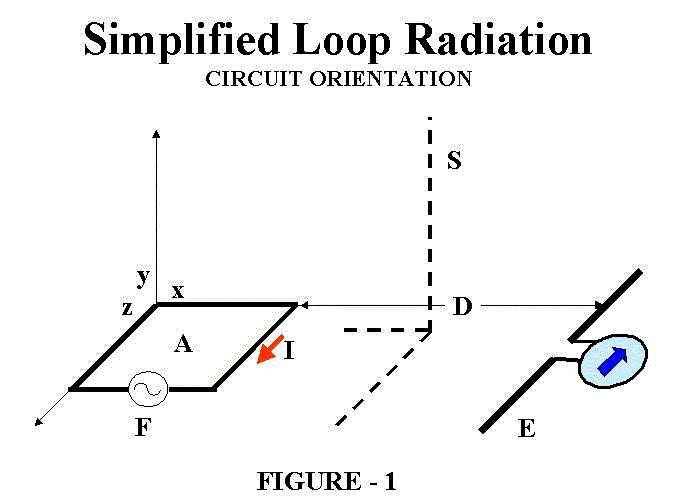
Refer to Figure 1 for a graphical illustration of these parameters. Discussion of the circuit characteristics related to this equation is very revealing:
Measurement distance ( r ) is dictated by the EMC specification, with commercial measurement distances ranging between 3 and 30 meters.
Radiated emission levels (e) created by active loops are proportional to the square of the frequencies, and linear for all other parameters. Since levels are increasing as the square of the frequency, it is very important to operate the circuit only as fast as necessary to process the data. As clocks have increased in frequency from 1 to 1000 MHz, the emission levels have increased by:
dB = 20 Log (1000/1)2 = 120 dB
Drive current (I) and switching frequency (F) (i.e. circuit bandwidth) are uniquely determined by logic family selection. Generally 9 to 11 harmonics are needed to adequately define the rise time for the signal. Generally, after logic family selection the designer loses control over the drive current and frequency.
Above the 9th or 11th harmonic frequency, low pass filters can be used to reduce circuit bandwidth, provided the waveform is not effected and compensation is made for the added propagation delay. Since the propagation time is Tp = ?(LoCo ), the blind application of filtering devices which change the transmission line L or C results in the deterioration of signal integrity.
Loop area (A) and shielding (S) are the only parameters totally under the designer's complete control. They are also the only parameters that do not effect the high speed operation of the PCB. Consequently, the major reductions of emissions come from reducing active loop areas and by the addition of shielding.
RADIATED SUSCEPTIBILITY COUPLING LOOPS
The same circuit can both radiate RF energy as well as be susceptible. For a small non-resonant loop oriented at angle (q), the induced voltage created by an incident plane wave is:
                    2p ε A sin (Θ)
          Vi (Θ) = ---------------       [Terman]
                         λ
By orienting the loop for maximum emission, sin (Θ) = 1; converting to frequency instead of wavelength, F(MHz) x λ(m) = 300 m/µS; and introducing the contribution provided by both the circuit bandwidth-frequency response, Bpb and shielding, S; the equation can be rewritten as:
                       0.021 ε F A Bpb
          Vi (max) = ----------------------
                           S


     Where:

     Vi (max) = Induced loop voltage (volts)
     ε  = Susceptibility field strength (V/m)
     F  = Susceptibility frequency (MHz)
     A  = Circuit capture area (sq meters), 0.1<(l/w)<10
     Bpb = Bandwidth-frequency response, In band Bpb = 1
     S  = Shielding effectiveness ratio
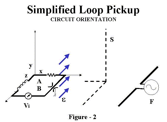
Refer to Figure 2 for a graphical illustration of these parameters. Discussion of the circuit characteristics related to this equation is also revealing:
Induced RF voltage is directly proportional to all parameters. When the induced RF voltage exceeds the noise threshold of the circuit, susceptibility occurs. This may be from RF overload or audio rectification.
Analog devices have continuous input/output transfer functions and are approximately 100 times (40dB) more susceptible than digital devices.
Although the narrowband electromagnetic field strength at each frequency could be the result of the environment, it is generally dictated by regulatory agencies. The most severe commercial radiated broadband electromagnetic field strength results from ElectroStatic Discharge (ESD).
Outside of the circuit passband, circuit RF attenuation determines narrowband signal response. Within the passband, narrowband signal response is essentially constant. On the other hand, broadband signal response is determined by both the circuit attenuation and bandwidth. Changing the bandwidth (BW) changes the coupled signal level by:
     dB = k Log (BW1 / BW0)


     Where:

     k = 10 for non-coherent signals
     k = 20 for coherent signals
Just as it was true for radiated emissions, it is also true for susceptibility loop coupling, i.e. loop area and shielding are the only parameters for which the designer has complete control. Consequently, major reductions in circuit susceptibility come from reducing the loop areas of the highest-bandwidth most-susceptible circuits and through the addition of shielding.
THREE STEP DESIGN STRATEGY
Examining the emission and susceptibility (immunity) characteristics of a loop permits us to be able to formulate a three-step design strategy for meeting the radiated EMC requirements. All three steps are inter-linked, and will be expanded in future articles.
1. Layout circuits to minimize high frequency loop areas. High-speed systems require high frequencies with broader bandwidths. Reduction of the area of the highest frequency circuit loops is the most important consideration. An easy way to accomplish this is to use multi-layer PCB's. They reduce circuit loop areas by as much as 40 to 60dB.
2. Minimize circuit bandwidth. Sometimes a major point of contention because reducing systems speed is not a popular option. Especially by marketing. However, many circuits are operating at high speeds or are using high-speed logic devices, when it is not necessary. Since radiated susceptibility increases with frequency and radiated emission increases as a function of frequency squared, using slower speeds (with reduced bandwidth) will desensitize the circuit to external susceptibility fields and will dramatically reduce emissions.
3. Shield problem circuits. This non-invasive suppression technique does an outstanding job of reducing both the radiated emission and susceptibility of a circuit. Since shielding is not inserted into the circuit it does not effect high-speed operation. In fact it is the only suppression technique that does not effect signal integrity.
REFERENCES:
J. D. Kraus, "Electromagnetics", 3rd Edition, John Wiley, NY 1984
F. E. Terman, "Electronics and Radio Engineering", 4th Edition, McGraw Hill, NY 1955
Return to START page
www.ronbrewer.com