COPYRIGHT (c) 2003 - ALL RIGHTS RESERVED
Ron Brewer
FUNDAMENTALS OF PCB EMC DESIGN
If the EMC characteristics of your electronic system aren't meeting your expectations, check the printed circuit board (PCB). After all, the active devices that accelerate the electrons and create our EMC problems are all located there. It's not widely known, but good PCB design can provide up to 50 dB reduction in both emissions and susceptibility, without any significant additional cost. It can't be over stated . . . good PCB EMC design is our most important design element.
Because power and signal distribution technology has advanced so significantly since the point to point schemes used in the wiring of vacuum tubes and early transistor based circuits, the older design techniques do not work to solve today's EMC problems! In the past, PCB technology focused on high production automated circuit manufacturing and uniformity. Uniformity was especially important with the front-end RF circuits of radios and televisions. Even then, these RF signals were low level and narrowband and except for the input signal and local oscillator circuits, these early PCB's were not operating at particularly high frequencies. Today, however, the increased currents, higher speed broad band signals, and smaller board dimensions make PCB design for EMC absolutely necessary in order to meet both regulatory and functional requirements.
In most cases PCB dimensions are several times greater than the harmonic wavelengths of the signals being propagated on the board, forcing us to design each trace as a transmission line. As an example, the propagation wavelength of the 10th harmonic of a 600MHz CPU clock in a PCB with a dielectric constant of 5 is only 4.5 inches . . . and many CPU's are running much faster than this.
 Currents move from a source to a load and then return back to the source forming small loop
antennas that are quite effective at these higher frequencies. The loop efficiency increases with
increasing frequency and loop area. As illustrated in Figure 1, layout must be considered
because it plays such an important part in EMC design.
Currents move from a source to a load and then return back to the source forming small loop
antennas that are quite effective at these higher frequencies. The loop efficiency increases with
increasing frequency and loop area. As illustrated in Figure 1, layout must be considered
because it plays such an important part in EMC design.
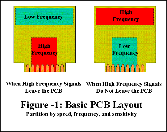
High-frequency devices should be segregated from low-frequency devices and positioned as close as possible to the backplane and connectors. Conversely, they should be positioned as far as possible from the backplane and connectors when high-frequency signals don't leave the board. A minimum of two inches is generally adequate. The increased spacing reduces the effects of capacitive and inductive coupling and helps prevent low-frequency circuits from being contaminated by high frequency signals.
There are four principal circuit loop categories: low-level analog circuit loops, high-level analog and digital circuit loops, analog power circuit loops, and digital power circuit loops. Because most of these loops are synchronously driven, and 80 to 90% may be active at one time, layout and bandwidth control is critical in order to achieve the desired 100+/-20dB reduction in RF emission and susceptibility (immunity).
Analog Circuits
Typically, low-level analog circuits appear as narrowband filters coupled to small signal amplifiers. High-level analog circuits are typically narrowband oscillators with approximately sinusoidal outputs. In both cases the circuits are steady state. As a result, except for the conducted switched mode power supply noise from associated power circuits, analog circuits are normally not responsible for problem emissions from PCB's.
Because they have a continuous input/output transfer function, any RF noise that exceeds the barrier potential of the many PN junctions in the semiconductor material of the various analog device's could be a susceptibility signal. Susceptibility occurs either from base band noise coupled directly to and within the circuit's passband or from audio-rectification where the modulation envelope of an RF carrier picked up by the circuit is recovered and then processed by the circuit.
Digital Circuits
The same susceptibility problems may occur with digital devices, but since analog devices are 100 to 1000 times more sensitive than digital devices, we normally associate this problem with analog devices. Analog power circuit loops tend to be quiet because analog circuits are steady state.
Digital circuits are noisy! Very noisy! So are their power circuits! The digital circuit's on and off behavior creates very fast trapezoidal signal waveforms. These waveforms are made up of the fundamental, which determines pulse width, and an infinite number of odd and even harmonics of varying phase relationships which dictate the waveform and determine rise time. Fortunately for both EMC and circuit operation, we do not need all of the harmonics. The first 9 or so will do. The rest we can eliminate, or at least try to. To make matters worse, the power supply output current follows the signal response as well.
Even though we may think differently, the power supply output is not supply steady state DC during circuit operation and must also be designed as a high frequency circuit. EMC design for high frequency circuits (for both emission and susceptibility) requires that the circuit layout minimize the RF coupling loop areas. The highest frequency loops should be kept as small as possible.
Two-Layer PCB's
For power distribution on two-layer boards, loop areas are minimized by keeping the power rails as close together as possible and by placing decoupling capacitors close to the culprit active components that need suppression. Decoupling capacitors do a good job for lower frequency circuits that are not operating at more than 5 times the self-resonant frequencies (SRF) of the capacitors. One way to extend the frequency range of a decoupling capacitor is to parallel the larger capacitor with a small value capacitor having low lead inductance. This improves the decoupling at frequencies greater than the SRF of the smaller capacitor, but sometimes makes the decoupling worse in the frequency range between the SRF's of the two capacitors.
SRF is largely determined by lead inductance, so anything that reduces lead inductance (shorter and wider) will increase the SRF and lower the RF emissions from the circuit. The use of a bus power distribution results in approximately 15 dB improvement in both the emission and susceptibility of the PCB. The bus does this by reducing the rail inductance and providing a high quality small value decoupling capacitance across the rails, reducing both the power and signal distribution RF impedance while increasing the SRF.
This technique is embodied in the multi-layer PCB and responsible for its success. In this case, the small value decoupling capacitance created by the configuration lies between the power planes and has valures that range from 50 to 1,500 pF/in.2 (depending on spacing and dielectric), and has virtually no lead inductance.
If you have already read the article on RF coupling loops, you are probably well aware that to control both radiated emission and susceptibility (immunity) of the high frequency circuit loops, it is important to minimize, minimize, and minimize. First, and most important, is the processing speed. This is accomplished by selecting and operating devices just fast enough to do the job on time. From an EMC perspective, this means that it is better to operate circuits in parallel to obtain the required through-put than to use HS serial processing.
Since high-speed is also synonymous with broad bandwidths, we must carefully control the bandwidth because radiated susceptibility increases directly with frequency and radiated emission increases as a function of frequency squared. Although not a popular option, using slower speeds (with reduced bandwidth) will desensitize the circuit to external susceptibility fields and will dramatically reduce emissions. In any case circuits should not be operated any faster than necessary
Starting with the highest frequency circuits, loop areas should be minimized. This may not be easy, but keep in mind that the multi-layer configuration reduces circuit loop areas by as much as 40 to 60dB. Circuit bandwidths should be reduced (using low pass filters). The limiting factor on bandwidth reduction using low-pass filters is the added delay. With TTL devices and clock speeds under 30MHz, this approach cures our headaches most of the time. When it doesn't, we may also have to add shielding. Shielding can be thought of as simply a high pass filter that is used to minimize the radiated field. The broadest frequency range of attenuation results from combining filtering and shielding.
Refering to Figure 1, the signals from high frequency circuit loops may be contained on the PCB or they may leave. When the signals are confined to the PCB, the circuit loops should be kept at least 2 inches away from any I/O circuits, especially the connectors. This reduces both the inductive and capacitive coupling into the I/O circuitry.
On the other hand, when the high frequency signals leave the PCB and go elsewhere via connectors, back-planes, or cables their circuits should be placed close to the connectors or back planes. If they are placed further away, longer traces are required to bring these high speed signals to the connector. This increases their loop area without changing their associated connector or back-plane coupling. Since these circuits are hard wired to the connectors, we can't have any better coupling than that! This is especially important for two layer PCB's where there are no signal reference planes.
Multilayer PCB's
The extra strength solution is the multilayer PCB! It's not the cure-all for EMC headaches, but it goes a long way toward being a universal cure. Multilayer PCB's have the greatest parts density because they reduce the number of signal returns and all but eliminate power conductors, enabling the designer to reduce the size of various circuits on the board as well as its overall size. This is especially important in reducing propagation delay, keeping loop areas small, and minimizing the size of any required PCB mounted shields.
The integral ground plane also makes possible the use of RF devices such as low-impedance microstrip and stripline transmission lines, waveguides and imbedded coaxial lines, and inductors/capacitors. The impedance of these integrated RF devices can be tuned to minimize normal and forward/backward crosstalk, and reduce reflections from terminations.
Compared to a two-layer PCB, a simple four-layer PCB using microstrip signal distribution will provide approximately 30 dB improvement in EMC performance. The is accomplished by lowering the power distribution impedance and reducing the signal loop area.
The power plane impedance is given by:

	   120 pi (h/W)
Zo = ------------------
		 e 0.5

Where:
	h = separation between stacked planes or trace and plane
	W= Width of plane or trace
	e = dielectric constant
Note: This equation is exact for h/W>15
From the equation, we can see that making the planes wide and bringing them close together will reduce the power supply impedance. Since the signal return is via the power return plane, running the traces over the power supply return plane reduces the signal loop area by several orders of magnitude. It also rotates the plane of the loop so that it is normal to, rather than coplanar with the PCB.
The microstrip impedance is also a function of its h/W ratio and can be modified easily by changing the trace width. Unfortunately the loop is still on the surface of the PCB, and although the loop area has been substantially reduced, it is still subject to both emissions and susceptibility problems.
Stripline reduces these problems. It is in essence, a shielded microstrip line formed by adding a ground plane over the microstrip. Clocks and other high-speed lines should be run as stripline. Stripline allows us to raise the EMC performance to 45 dB when compared to a two-layer configuration.
If the entire PCB could be configured as stripline, the components themselves would be the worst offenders. The principal component problem is lead inductance and this can be reduced by using surface-mount devices. Surface mounted components in a stripline-configured PCB will provide approximately 6 to 8 dB of additional attenuation. Flip chips or ball grid arrays (BGA) will add a few more.
The internal ground plane that makes microstrip and stripline configurations possible also provides inherent shielding and isolation of signal layers. Typical isolation between signal layers separated by a ground plane is in the order of 50 to 55 dB. This level of attenuation is very effective in reducing crosstalk between sensitive circuits and can be used to nearly eliminate forward and backward crosstalk. This high level of attenuation between isolated signal planes however necessitates the use of co-located signal-return vias whenever signal traces have to be run between isolated signal planes.
Shielding
Ground planes can also act as image planes or as one side of a PCB-mounted shielded enclosure. PCB shielding is a non-invasive suppression technique that does an outstanding job of reducing both the radiated emissions and susceptibility of a circuit. Since the shielding is not inserted into the circuit it does not effect high-speed operation. In fact, it is the only suppression technique that does not effect signal integrity. Shielding could be used as a stand-alone solution to the EMC problem, but it would have to provide the entire 100 dB or so of attenuation. Not impossible, but certainly not nearly as efficient as first designing the PCB to provide 45 to 50 dB of attenuation and then adding 45 to 50 dB with shielding.
Return to START page
www.ronbrewer.com