COPYRIGHT (c) 2003 - ALL RIGHTS RESERVED
Ron Brewer
SIGNAL INTEGRITY - A NEW NAME FOR AN OLD PROBLEM . . .
RFI, BCI, TVI, EMI, EME, EMF, EMS, ESD, EFT, EMP, and #@$%&! are some of the many acronyms used to denote different facets of Electro-Magnetic Compatibility (EMC). SI (Signal Integrity) is yet another! EMC has two parts. The first, inter-systems EMC, addresses a systems ability to operate within its external environment and determines its compliance with governmental EMC requirements. Inter-systems EMC includes both design compatibility (radiated and conducted emission and susceptibility) and operational compatibility (frequency, amplitude, separation, and time management). The second, intra-systems EMC, addresses the internal RF/signaling characteristics that effect a systems functional operation, performance, and reliability. This is sometimes described under the heading of self-compatibility. The internal RF sources that create most intra-systems EMC problems also create the inter-systems emissions problems.
The principal effect of intra-systems EMC problems in high-speed digital systems is signal-timing variation caused by waveform distortion, crosstalk, non-monotonic signaling, device I/O capacitance differences, ground bounce, and simultaneous switching noise. Digital systems designers lump these primarily analog intra-systems EMC problems together under Signal Integrity. Understanding the basics of signal integrity will help designers minimize changes occurring late in the design cycle (during those crisis's to meet governmental EMC requirements: FCC, EU, MIL-STD-461, etc.) that may degrade operational performance. Just being aware that signal timing may be adversely effected by indiscriminately adding EMC suppression components is a big step. This article does not cover all aspects of signal integrity, only the principal ones effected by adding suppression components to an otherwise fully functional system.
Recognizing timing problems.
The most important elements of signal integrity are timing!, timing!, and timing! Intended signals need to reach their destination at the same time all the time. If an unintended signal (i.e. internally or externally coupled noise) reaches the destination first, changes the signal rise time, or causes it to become non-monotonic, it's a timing problem. If added suppression components distort the waveform, change the signal rise-time, or increase delay it's still a timing problem. It's easy to visualize that circuit design, parts placement, and trace routing effect timing. It's not so easy to visualize that trace-width variations, PCB dielectric, receiver input sensitivity, transmission line termination, fan-out, crosstalk, EF/HF radiation, and suppression component selection, among other things, also effect timing. And with today's high-speed circuits, timing is critical!
How much timing variation can be tolerated.
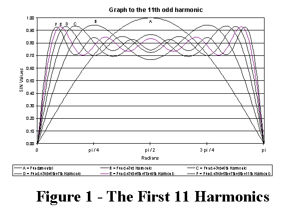 A 500MHz clock requires a bandwidth of 5 GHz and completes one cycle in 2
nanoseconds. Very fast! The fundamental determines the pulse width. The rise time
establishes the pulse bandwidth and edge rates and is determined by the number of
harmonics. In general, 9 harmonics (or so) are required to establish the rise time. This
relationship is illustrated in Figure 1. Because there is little change in rise time as we add
more harmonics, the amplitudes of the higher frequency harmonics should be reduced. A
500 MHz clock pulse can be approximated by a 50% duty cycle trapezoidal waveform of
1000 ps duration with a worst case rise time of: Tr = 500 ps (not much of a trapezoid) or
more typically a rise time of approximately: Tr = 250 ps. Because clock edge rate is used
to synchronize a system's numerous logic circuits, threshold crossing time, clock jitter,
and clock/signal arrival time (skew) is very important. Delay is analogous to reducing the
clock speed and must be minimized. Skew should not exceed 10% (or less) of the clock cycle
time. For a 500MHz clock this means under 200 ps.
A 500MHz clock requires a bandwidth of 5 GHz and completes one cycle in 2
nanoseconds. Very fast! The fundamental determines the pulse width. The rise time
establishes the pulse bandwidth and edge rates and is determined by the number of
harmonics. In general, 9 harmonics (or so) are required to establish the rise time. This
relationship is illustrated in Figure 1. Because there is little change in rise time as we add
more harmonics, the amplitudes of the higher frequency harmonics should be reduced. A
500 MHz clock pulse can be approximated by a 50% duty cycle trapezoidal waveform of
1000 ps duration with a worst case rise time of: Tr = 500 ps (not much of a trapezoid) or
more typically a rise time of approximately: Tr = 250 ps. Because clock edge rate is used
to synchronize a system's numerous logic circuits, threshold crossing time, clock jitter,
and clock/signal arrival time (skew) is very important. Delay is analogous to reducing the
clock speed and must be minimized. Skew should not exceed 10% (or less) of the clock cycle
time. For a 500MHz clock this means under 200 ps.
Signal propagation time in a dielectric.
In a vacuum, signals travel with a velocity: Vv = C = 3*10^8 m/sec. Within PCB's however, the velocity is reduced by the dielectric. The velocity in a dielectric: Vd = C / (er)^0.5 m/sec. Trace propagation time is the inverse of the velocity: Tpd = (er)^0.5 / C sec/m. This equates to Tpd = (LC)^0.5. This last expression is very important! It indicates that any series or parallel inductive or capacitive suppression components applied to PCB traces or logic devices will increase delay. On high speed PCB's, signals are distributed using either microstrip (signal trace located on the PCB surface above its return plane) or stripline (signal trace located between two return planes). For FR-4 material with (er) = 4.7, stripline propagation time Tpd = (4.7)^0.5/3*10^8 = 7220 ps/m or 180 ps/inch. This is approximate, because (er) varies locally within a PCB and from one PCB to another.
High-speed signal traces are transmission lines.
Continuing with the 500 MHz example, the fundamental wavelength in FR-4 material is 11.07 inches (Wave length = C / [F * (er)^0.5]). For a CW signal, the concern would be standing waves as the trace dimension reached 1/4 wavelength. For a pulse, the concern is the critical line length (CLL) determined by the rise time. CLL = Tr / (2.5 * Tpd). For a rise time Tr = 250 ps and propagation delay/unit length Tpd = 180 ps/inch, the CLL = 0.5 inches. One-half inch! This is the length where transmission line effects become significant and the line terminated in its characteristic impedance. Doing this creates a "flat" transmission line with maximum power transfer and no troublesome reflections. Under matched conditions, increasing the transmission line length only increases the delay and attenuates the signal amplitude; it does not significantly change the waveform. In general, only one end needs to be terminated to reduce waveform distortion, but the timing for intermediate points will depend on which end is terminated. With load termination, the incident signal is matched. With source termination, the signal is matched when its reflection returns to the source.
Proper transmission line termination is important.
 Incorrect termination impedance can result in ringing (oscillatory behavior from excess
inductance) or signal roll-off (attenuation of higher frequencies from excess shunt
capacitance) and can prevent driver outputs from reaching associated receiver switching
levels. Ringing can cause non-monotonic behavior e.g. the signal crosses the switching
threshold several times. Depending on phase relationships, crosstalk and external EF/HF
field coupling can also cause non-monotonic behavior and change signal timing. Figure 2
illustrates how this occurs. Non-monotonic behavior of clock lines is critical because of
multiple clocking. This is not quite as big a problem with data lines. Other side effects of
ringing are increased EF radiation and line-to-line crosstalk. Roll-off on the other hand,
results in increasing the rise time and associated delay of the line. This generally reduces
EF radiation at the higher frequencies and reduces line-to-line crosstalk. It also increases
signal delay and reduces systems throughput.
Incorrect termination impedance can result in ringing (oscillatory behavior from excess
inductance) or signal roll-off (attenuation of higher frequencies from excess shunt
capacitance) and can prevent driver outputs from reaching associated receiver switching
levels. Ringing can cause non-monotonic behavior e.g. the signal crosses the switching
threshold several times. Depending on phase relationships, crosstalk and external EF/HF
field coupling can also cause non-monotonic behavior and change signal timing. Figure 2
illustrates how this occurs. Non-monotonic behavior of clock lines is critical because of
multiple clocking. This is not quite as big a problem with data lines. Other side effects of
ringing are increased EF radiation and line-to-line crosstalk. Roll-off on the other hand,
results in increasing the rise time and associated delay of the line. This generally reduces
EF radiation at the higher frequencies and reduces line-to-line crosstalk. It also increases
signal delay and reduces systems throughput.
Signal delay from device I/O capacitance and suppression components.
Both microstrip and stripline inductance and capacitance are principally related to the length and width of the trace. Thickness of the trace has little effect. For a 10 mil stripline centered between two planes 20 mils apart, the capacitance is approximately 50 pF/foot (i.e. 4.166 pF/inch). Since Tpd = (L * C)^0.5 = 180 ps/inch, L = 7.78 nH/inch. Input capacitance variation for CMOS devices typically ranges from 2 to 7 pF. Not much, but consider what happens to the delay. For a short 1 inch line with no additional capacitance the delay is 180 ps. For the same 1 inch line terminated with a 2 pF part, Tpd = (7.78 * 10^-9 * 6.166 * 10^-12)^0.5 = 219 ps. With a 7 pF part, Tpd = (7.78 * 10^-9 * 11.166 * 10^-12)^0.5 = 295 ps. There is 76 ps variation in timing between parts with 115 ps additional delay resulting from the 7 pF capacitance.For a longer 10 inch line with no additional capacitance the delay is 1800 ps. The same line terminated with a 2 pF part, Tpd = (77.8 * 10^-9 * 43.66 * 10^-12)^0.5 = 1843 ps. With a 7 pF part Tpd = (77.8 * 10^-9 * 48.66 * 10^-12)^0.5 = 1946 ps. There is now 103 ps variation in timing (rather than 76 ps) between the same parts. Plus there is now 146 ps delay resulting from the 7 pF capacitance (an increase of 31 ps). The longer the trace the worse the problem! With Monte Carlo analysis the timing differences from component variations can be resolved. Not easily -- but it can be done -- and the systems timing adjusted accordingly. Keep in mind the effects of fanout must also be considered. Woe to the engineer that just slaps a little 100 pF capacitor across the line to solve an EMC problem. Now the delay at the 7 pF part becomes: Tpd = (77.8 * 10^-9 * 148.66 * 10^- 12)^0.5 = 3401 ps! The same thing happens when that little 300 nH ferrite bead is placed in series with the line! In this case: Tpd = (377.8 * 10^-9 * 48.66 * 10^-12)^0.5 = 4288 ps delay! It may not be obvious from these calculations, but this added delay (7 to 12 times the skew requirement) will result in increased logical failures (if it works at all) and necessitate re-budgeting the systems timing. Yes, the EMC problem may be solved, but turning the system off would solve the problem just as well!
A follow-up on using suppression components.
The EMC solutions approaches that have been used in the past on low-speed systems may cure today's emissions and crosstalk problems, but introduce signal integrity problems that result in high-speed system failures! This is one of the primary reasons why EMC hardening should be designed into the system from the beginning and not applied after the system design is completed! This does not mean that suppression components cannot or should not be used to solve EMC problems in high-speed digital systems. It's a matter of when and how! There are five basic types of components with amplitude-frequency or amplitude-time characteristics that are used for suppression, i.e.: ferrites and high frequency filters, high frequency low inductance capacitors, transient suppressors/zener diodes, current limiting resistors, and shielding. Used properly they work well . . . but they should not be used indiscriminately.With the exception of shielding, each of these devices is inserted into the signal path and has intentional or parasitic series inductance and/or shunt capacitance that may result in signal integrity problems. Even the resistor! So long as the effects, of this reactance on the systems operation, are understood and considered during design; suppression components can be planned for (just in case) or used to reduce unwanted emissions and susceptibility. Shielding is used for the same purposes, and from the viewpoint of signal integrity is quite unique. Since shielding is not inserted into the circuit, it does not effect circuit operation, and can thus be used at any time to solve emission and susceptibility problems without impacting signal integrity. It is the only suppression component/technique that can be used this way.
Return to START page
www.ronbrewer.com